 Hello, readers welcome to the new post. In this post, we will learn DIfference between Double-sided and Multilayer PCB boards. The word PCB stands for printed circuit board, it is a circuit board that is used for the construction of different circuits on this board the substrate at which different paths are designed by the copper for the connections of different components used for the circuit. With the creation of this circuit board, our complicated wiring system for the production of circuits has been eliminated. This circuit board is now used in almost every electronic component like from calculators to different devices used in medical industries consisting of PCB.
There are many types of PCB according to their use and construction such as single-sided PCB, double-sided PCB, Flexible PCB, Rigid PCB, Rigid-Flex PCB, etc. In today’s post, we will look at the multilayer type of printed circuit board and double-sided PCB. Numerous PCB suppliers are working in this universe. Here I want to mention that the best and most reliable PCB supplier comes with different types of PCB boards such as single-sided, and double-sided rigid PCB. With that PCB they also offer multilayer PCBs with affordable prices that can easily get for anyone. The best PCB supplier is PCBWAY. PCBWAY comes with these boards and provides all the needed requirements for a single platform. PCBWay offers standard PCB, they can help to produce 2-14 layers, even more layers for choosing advanced PCB. You can get HDI for 4-layer or more. Through-hole board PCB is offered in advanced PCB with IPC 6012 class 2. Layer advanced up to thirty layers can get. Standard PCB in material FR-4, Aluminum, and Rogers can get. In standard PCB you can get solder masks in colors Pink gray orange and transparent solder masks with Black FR4 also available.
To get the board just have to send the Gerber to the PCB team. They will get the detailed overview and make according to that information and will send your boards in a given time interval. All in all, they not just offered the PCB boards but also high-level standards that everyone needs to meet. So I recommend you to get the boards for your different projects So let’s get started.

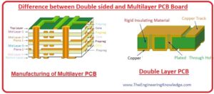
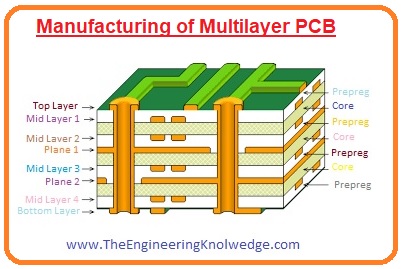
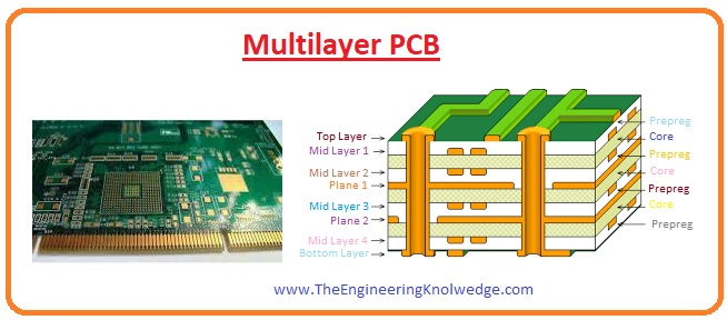
What is Multilayer PCB
- Multilayer PCB comes with 3 or more layers that have conductive paths. There is insulation materials is applied between layers to provide safe working and connected with the use of adhesive materials.
- The structure of these boards comes with upper and lower layers like double-sided boards and has more layers on both sides.
- The layers of boards are connected with copper-plated holes and there can be about 40 layers for multiple boards.
- For the creation of a circuit different active and passive components are connected on the upper and lower layers of the board and internal stacked layers are used for routing features.
- Now commonly used boards with multiple layers are 4 to 12-layer boards that have features to handle a larger number of components.
PCB Via
- Via is the electrical connection used for the connection of layers on multiple layer boards. They are small-sized holes on board and pass through two or more neighboring layers.
- Vias are plated through holes since used for the connection of through-hole components on board and come with larger dimensions as compared to vias. The via holes are covered with copper for providing electrical connection in insulating materials there separating layers of the board.
- Based on applications board needs vais over all layers or on external layers
Multilayer PCB Disadvantages
- Now we describe some drawbacks of this PCB you must be aware of these disadvantages with the benefit of this board.
High Cost:
- The production prices of these boards are higher than single and double-sided boards due to complications in the process. It needed large machine work and skills for the assembly process.
Complex Production:
- There is a need for more time for the manufacturing of boards and also designers need that have skills for the creation of board.
- The use of lamination and substrate base don active and passive connected components.
Creation Time:
- As we discussed above its manufacturing is very complicated and needs special care so it takes a long time for its creation
Double-Sided PCB Board
- The creation of a double-sided board has the same steps as a single-sided board. The difference is that using a single-sided core started with copper on both sides.
- At the time of manufacturing drill holes are made called vias they are plated with conductive materials or non-conductive materials.
- The current flows from one side of the board to another side through vias. Double-sided boards come with a high cost as compared to single-layer boards and lower than multiple-layer boards.

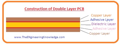
Construction of Double Layer PCB
- In this board base material is FR4, aluminum, or also plastic used. A thin layer of copper laminated exists on both sides. The upper foil is copper and solder mask layers are used that insulate copper to make connections with other metals or conductors.
Double-sided PCB Board Applications
- Due to its simple design and ease of handling, some practical applications of this board are described here.
- The use of this board in technical devices is also employed in medical devices like X-ray machines, CT scans, and pacemakers consist of this circuit board.
- In industries, this board also has numerous applications in different machines and instruments.
- In different power converter circuits, it is used.
- Different converters like analog to digital or digital to analog use printed circuit boards for their circuit assembly.
- Different control relays are also comprised of this Pcb.
- In HVAC heating, ventilation, and air conditioning this board is also used.
Read also:
- What is PCB Leds Circuit Board: What Do You Need to Know
- Purple Solder Mask Printed Circuit Board in 2$
- Applications of Multilayer PCB
- Advantages of Multilayer PCB
- Construction of Multilayer PCB
That is all about the Difference between Double-sided and Multilayer PCB boards. Further, you can get quality boards from PCBWAY. Thanks for reading Read our More Engineering Blogs


