Hello, readers, welcome to the new post. In this post, we will discuss the construction of multilayer PCB. PCB is a very important and main part of electronic projects and instruments, and no device can be created without this module. Over the board, all components of any electronic project and device are placed and linked in the circuit. There are traces of copperawn over which circuits and symbols of the different components are assembled to make the project.
Many PCB providers are functioning in this world. Here I want to explain about the best PCB supplier that comes with different types of PCB boards, such as single-sided and double-sided rigid PCB. With that PCB, they also offer multilayer PCBs with reasonable charges that can easily be for anyone. This greatest PCB provider is PCBWAY. PCBWAY comes with these PCB boards and offers all desirable necessities for a single platform.
PBWAy offers standard boards and helps to make board layers from 2 to 14 layers, and they also provide advanced boards. They also offer an HDI board with four layers or more. They also have supported advanced PCB with IPC 6012 class. In advanced layers, they can provide 30 layers. The standard board comes with materials such as FR4, aluminum, and Rogers. For standards board, they also provide solar maks with pink, grey, orange, and transparent solder masks with black FR4. PCBWAY also provides project services from start to finish points and they have a lot of staff to provide quality services.
In this post, we will have a detailed construction of multilayer PCB, features, advantages, and other parameters. So let’s get started.

What is Multilayer PCB?
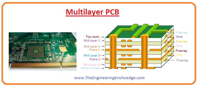
- Multilayer boards have two more layers and have features to provide current conduction and connection.
- Normally the number of layers for these boards is four, eight, and so on.
- The board design is complex, and the arrangement of layers in this board is like a double-sided board with different stakes. Layers on these boards are configured layers that are connected through holes of copper plating.
- The use of multilayer board boards provides different features for different industries and machine devices.
- The advancements with time provided electronic, and some circuits needed complicated boards.
- Single- and double-layer use in different projects causes some issues such as noise crosstalk and stray capacitance and cannot handle large projects of engineers considering introducing the multilayer PCB board.
- These boards come in four- to 12-layer combinations according to users’ demands.
Construction of Multilayer PCB
- There are certain types of processes, and care is needed to make this complicated circuit board to avoid the circuit mixing interlinking of connections.
- To make the PCB, there is a special arrangement of machines and instruments used.
- Mian steps for the construction of multilayer PCBs are explained here.
- First of all, the design of the board is created through the use of different types of software, such as Proteus, Eagle, etc.
- After that internal layer, the core is created, and a laminate of the required dimensions is created with the use of a copper sheet.
- Now lamination is done through the internal layer of prepeg foil and sheets of copper.
- In this stage, the staking of layers is done in different steps, such as the lower layer through the copper sheet, then prepreg sheets, internal layers, then prepreg here, and at last, the copper sheet placed at the upper side.
- At last, pressure is applied through the use of a hydraulic press machine. To remove the air, there must be a vacuum created.
Factors Affecting Manufacturing Multilayer PCBs
- There are some points you must keep in mind during multilayer PCB construction. Such as power integration and signal integration.
- Current can flow through copper traces but at limited value, meaning it offers some value of resistance to larger current.
- There is the usage of control impedance traces. To bear the large value of temperatures, the thickness of copper in traces should be large.
- The width of the temperature of traces should change according to configuration.
- There are no vertical traces to avoid the phenomenon of electromagnetic induction.
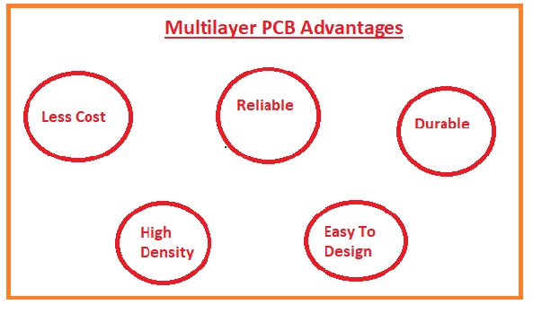
Multilayer PCB Advantages
- The main advantages of multilayer PCB are listed here with the details.
- Its main benefit is that it exists and is created in a smaller size than other boards. Due to its small size, it is used in laptops, mobile phones, and tablets.
- Its design is lighter and used in different types of projects due to its lighter weight.
- It also offers features of high quality over the other boards and is reliable for different projects.
- Its durable and long-life operation makes it effective for different projects. Has the ability to work in high-temperature and pressure conditions.
- There are features of high density offered by the board.
- It also has features to work as one module without the combination of other boards.
Multilayer PCB Disadvantages
- The main disadvantages of multilayer PCB are explained here.
- Due to the difficult design and requirement of special equipment, its cost is larger than other boards.
- Its construction is more complicated than other boards and needs careful techniques for making this board.
- As some companies created this board, its availability is less.
- Due to the complicated design, there is a need for a skilled person to make it.
Comparison between Single Layer and Multilayer PCB
- Single-layer PCB is less dense, while multilayer PCB has high density, and high density makes multilayer PCB effective for different projects.
- The size of a multilayer PCB is less than a single-layer PCB, and these features make it useful in small-size devices such as mobile watches and tablets. Multilayer PCBs are to be used in smaller devices, while high-capacity single-layer PCBs must be installed into larger products.
- The weight of the multilayer PCB is less than the single-layer PCB.
Multilayer PCB Applications
- There are different uses of this board according to design and structure
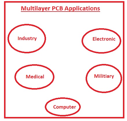
- Its small size and less weight make it useful in the construction of smartwatches.
- It is used in laptops, mobile tablets, etc.
- It is used in telecom such as in devices used for signal transmission, and satellite.
- In industries, different devices are created with the use of this board.
- Medical instruments are created with this board.
- In the military, there is different instruments are created with this board.
Read also:
- Applications of Multilayer PCB
- Advantages of Multilayer PCB
- Difference Between Single Sided PCB & Multilayer PCB
- Difference between Double sided and Multilayer PCB Board
- Multilayer PCB, Construction, Working, Types & Applications
That is all about the Construction of Multilayer PCB. I have explained each parameter related to this tutorial. i hope now you have a detailed understanding of this board. For further queries ask in comment. Thanks for reading have a good day.Read our More Engineering Blogs


