 Hello friends, I hope you all are doing great. In today’s tutorial, we will have a look at Introduction to Multistage Amplifiers. In numerous amplifier circuits application, the results obtained from a single amplifier configuration is not enough. To make results more accurate more than one amplifier is configured that configuration is known as a multistage amplifier.
Their arrangements is such that the output of first amplifier is linked with the input of the second and the output of 2nd is connected with the third input and continues. In today’s post we will have a detailed look at its circuit, working, and other parameters. So let’s get started with the Introduction to Multistage Amplifiers.
Introduction to Multistage Amplifiers
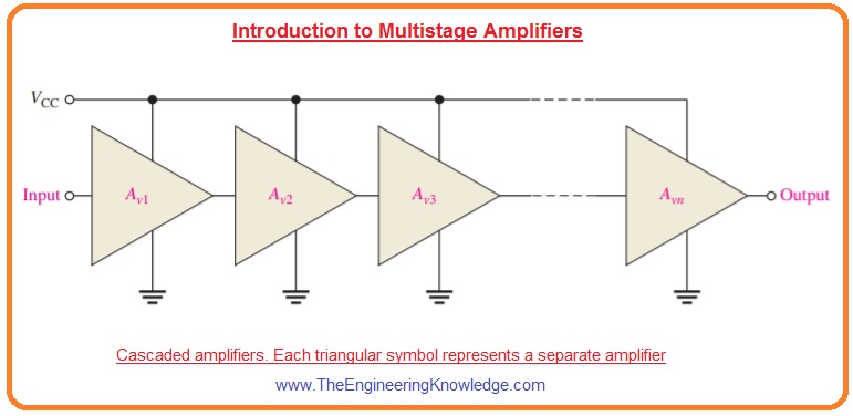
- The multistage amplifier are constructed with the series connection of more than one amplifier in a single casing the output of one amplifier is used input for others.
- Every amplifier in this configuration is known as one stage. So as single multistage amplifier has more than one stage.
- Each amplifier in this arrangement performs its separate process of amplification.
- So the output of this circuit is amplified much time according to a number of amplifiers in circuits.
- The overall voltage gain A’v for single multistage amplifier is shown in the below figure and is multiple all voltage gains of amplifiers.
A’v =Av1Av2Av3…….Avn
- The voltage gain of an amplifier is defined in decibels or dB as mentioned here.
Av(dB)= 20 log Av
- For a multistage amplifier, it will be sum of all amplifier used in a single casing.
A’v(dB) = Av1(dB) + Av2(dB) + ….. + Avn(dB)
Capacitively Coupled Multistage Amplifier
- To explanation in below figure 2 stage amplifier capacitively coupled is shown.
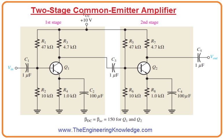
- You can see that both circuits are common emitter amplifier configuration the output of the first circuit is given to the second circuitry through the capacitor.
- The use of the capacitor stops the dc biasing of one stage to get effects from the second circuit but permits ac voltage to pass without attenuation as XC is almost zero ohms at the frequency of operation.
Loading Effects
- To calculate the gain of the first circuit stage we must take into consideration the loading effect of the second.
- At frequency coupled capacitor C3 operates as short circuit the total input resistance of a second amplifier or stage work as output for the first stage.
- By observing from the collector of transistor Q1 the 2 biasing resistances in 2nd stage R5 and R6 are in parallel combination with the input resistance at the base of transistor Q2.
- In simple words voltage at the collector of transistor Q1 appears at resistances R3, R5, R6 and Rin(base2) of second amplifier or stage and all these resistances are in parallel combination with the ac ground.
- So effective ac collector resistance of Q1 is equal to the total of all parallel resistances (R3, R5, R6 and Rin(base2)). It is shown in the below figure.
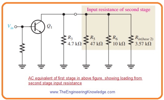
- The voltage gain of first stage is decreased with the loading of 2nd stage or amplifier as the ac collector resistance of the first stage is less than the value of collector resistance R3.
Voltage Gain of First Stage
- The first stage ac collector resistance is given as.
Rc1 = R3ΙΙR5ΙΙR6ΙΙRin(base2)
- We can verify that IE=1.05 mA r’e=23.8Ω Rin(base2)= 3.57kΩ. The value of effective collective resistance will be
Rc1=4.7kΩІІ47kΩІІ10kΩІІ3.57kΩ=1.63kΩ
- So base to the collector voltage gain of first stage is given as.
Av1=Rc1/r’e=1.63kΩ/23.8Ω=68.5
Voltage gain of second stage
- There is no load resistance for second stage so the ac collector resistance R7 and gain is given here.
Av2=R7/r’e=4.7kΩ/23.8Ω=197
- Compare gain of both stages and note that how much loading from the 2nd stage decreases the gain.
Overall voltage gain
- The overall voltage gain with no load is given as.
A’v=Av1Av2=(68.5)(197)=13495
- For instance, if a signal of one hundred microvolts is applied to the ist stage and if there is no attenuation exits in base circuitry due to the resistance of source the output from the second stage of (100uV)(13495)=1.25volts will come.
- The overall voltage gain can be defined in dB as below.
A’v(dB)=20log(13495)=82.6dB
Dc voltage in capacitively coupled Multistage Amplifier
- As both stages in first circuitry are the same so the value of dc voltages for transistor Q1 and Q2 is similar.
- As βDCR4>>R2 and βDCR8>>R6 the value of dc bias voltage for Q1 and Q2 will be.
VB=(R2/R1+R2)VCC=(10kΩ/57kΩ)10v=1.75v
- The value of the dc collector and emitter will be.
VE=VB-0.7V=1.05v
IE=VE/R4=1.05v/1kΩ=1.05mA
IC=IE=1.05mA
VC=VCC-ICR3=10V-(1.05mA)(4.7kΩ)=5.07v
Direct Coupled Multistage Amplifier
- In below figure basic 2 stage direct coupled amplifier circuit is shown.
- You can see that there is no coupled capacitor exits in this circuitry.
- The dc collector voltage of the first stage given as base bias voltage to the second stage circuitry.
- Due to direct coupling, this category of amplifier has a good frequency response than the capacitively coupled or bypass capacitor in which the reactance offered by the coupling capacitor at less frequency can become large.
- The enhanced reactance of capacitor at less value of frequency causes a reduction of gain in capacitively coupled amplifier.
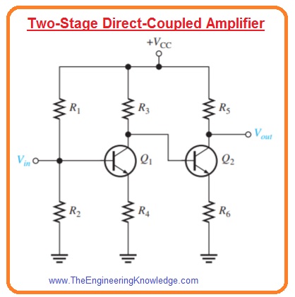
Advantage of direct coupled amplifier
- This type of direct-coupled amplifier can amplify less frequency value without reduction of voltage gain as there is no capacitive reactance that occurs in this circuitry.
Disadvantage of direct coupled amplifier
- Its drawback is that less variation in dc bias due to temperature variation effects or power supply changes are amplified by the following stages that cause high drift in dc level through the circuitry.
Read also:
- LM324 – Single Supply Quad Operational Amplifiers worksheet
- Difference Between An Operational Amplifier and Comparator
- Amplifier circuit using LA4440 IC
- Introduction to LM258 Dual Operational Amplifier IC
- Introduction to 2sc828 NPN Amplifier Transistor
So, friends, it is detailed post about Multistage Amplifiers if you have any questions ask in comments. Thanks for reading.