Hello, friends, I hope all of you are enjoying your life. In today’s tutorial, we will have a look at a double-sided PCB board. PCB stands for printed circuit board; it is a thin board constructed by epoxy, fiberglass, or some other laminated substance. On this circuit board, there are numerous paths that are manufactured for current movement, and numerous components for any circuitry can be assembled on these conductive paths. Components like resistors, transistors, capacitors, or other ICs can be assembled on this board.
This board has lots of practical applications in electronic devices and projects, like computers, laptops, mobiles, and calculators, which consist of this circuit board. An example of a PCB is its motherboard on which different components are assembled. There are numerous types of PCB according to construction and uses, like single-sided, multilayer, rigid, rigid-flex, flexible, etc. In today’s post, we will have a look at double-sided construction, its working, applications, advantages, and disadvantages. So let’s get started with what a double-sided PCB board is.
Double-Sided PCB Board
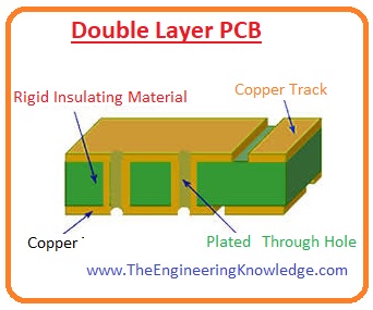
The double-sided printed circuit board is also defined as a double-layer board, as it provides conductive paths on both sides for the assembly of components.
On this circuit board, both sides are covered or coated with current-carrying (conductive) material like copper.
The main feature of this board over the single-layer board is that on this board there is a hole through which components of one side can be connected with the other side.
For the connection of components on this module, there are 2 methods used. The first one is surface-mounted, and the second one is through-hole. Both of these have their advantages and disadvantages and can be used according to the user’s requirements.
In the through-hole connection technique, the small wire is passed through holes and joins different components.
In the surface-mounted technique, there are no separate wires used to link components, but in this method, on the surface of the board, wire is already soldered to provide conductive paths. This method uses less space for component assembly and decreases the weight of the board.
Construction of Double-Layer PCB
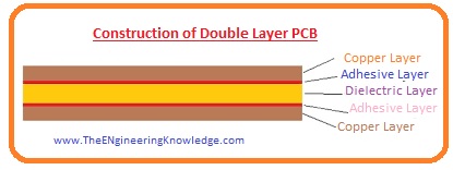
The construction of this circuit board is similar to the single-layer circuit board; its construction is described here in detail.
In this circuit, the substrate is manufactured by glass fiber or epoxy resins; the type of base material depends on the rigidity and flexibility of the board.
In this double layer, PCB over base substance copper lamination is done to provide conductive paths for components.
To protect the environment, both sides of the circuit board comprise a solder mask over the copper covering.
For an easy understanding of the circuit board for new users, there are different component symbols that are already designed on the board over the silkscreen that is above the solder mask.
Double-sided PCB Board Applications
Due to the simple design and ease of handling, some practical applications of this board are described here.
The use of this board in technical devices is also employed in medical devices like X-ray machines, CT scans, and pacemakers, which consist of this circuit board.
In industries, this board also has numerous applications in different machines and instruments.
Different converters, like analog to digital or digital to analog, like analog to digital or digital to analog, use printed circuit boards for their circuit assembly.
Different control relays are also comprised of this PCB.
In different power converter circuits, it is used.
In HVAC (heating, ventilation, and air conditioning) this board is also used.
Different lighting devices like light-emitting diodes consist of circuit boards.
Different power supplier circuits also consist of these PCB boards.
Voltage regulators also consist of this board.
UPS is a common useable device in our home and offices; it also uses PCB for circuit assembly.
Different traffic control circuits also comprise this module.
Vending machines also use this PCB board.
Your computer motherboard is also made with this printed circuit board.
Vending machines also comprise these boards.
Line reactor circuitry also uses this board.
- Printers also comprise this board.
- Your cell phone also consists of this board.
- Different amplifier circuits also consist of this board.
How Are Double-Sided PCBs Made?
First of all, the design of the PCB board was made with the use of different software
After completion of the design, the PCB layout is made. The PCB layout is printed on paper.
This material is selected for board creation. The selection of materials is based on design. The normally used material for PCB substrate is FR4; some boards use high-speed and high-frequency PCBs.
In this step, cutting of copper-clad laminate is done according to the size needed. CCLs are thin layers of copper foil laminated on the nonconductive substrate. The accuracy in cutting provides accurate measurements for further processing.
Now holes are drilled in the CCL to make sure proper vias and component holes are made. These holes are made based on the design and then help to connect different layers of the board.
Holes made in the previous step face electroless copper deposition. This involves coating holes at the inner side with the use of thin copper layers to make a conductive path between the top and lower layers.
In this step, photoresist material is used on the surface of CCL. The circuit pattern is applied on the photoresist with the help of a UV light-sensitive mask. When light strikes, chemical changes occur. Make a pattern for the next process.
A thin layer of copper is electroplated on the exposed CCL, and the circuit pattern is reinforced. This copper layer increases the conductivity of traces.
It is the etching step where a double-sided PCB is made with accuracy and a chemical process link for refining complicated circuit designs on copper-clad laminate. In pattern plating that comes with electroplating, an extra copper layer is applied on exposed parts of the board coated with photoresist material.
This automatic optical inspection is performed to check accuracy and reliability. The circuit pattern is etched on copper-clad laminate, and the PCB is put in for AOI inspection, which is the latest technique for finding faults.
At last, flying probe testing is performed to check the accurate working of the board.
Advantages of Double-Sided PCB Board
It is a basic PCB board that can be easily made.
It has copper layers on both sides for making the circuit.
Both side copper layers help to connect a larger number of components on the board.
It is a flexible nature board.
that provides high-circuit flexibility
It has a smaller size of the board due to the side layer configuration.
It is a low-cost board.
that helps to make complex designs
Single-Sided vs. Double-Sided vs Multilayer PCBs
Single-Sided PCBs
The single-sided board is also called a single-layer PCB, and this board has single layers where conductive layers are made. So a single side is used for component connections, low-cost projects, and circuit creation.
Different materials were used for the creation of these boards, such as paper-reinforced phenolic resin, copper foil, and glass fiber-reinforced resin. Single-sided boards are commonly made and used.
Double-Sided PCBs
Double-sided boards are almost the same as single-sided, but the difference is that double-sided has conductive layers on both sides. So a larger number of components are connected on both sides for circuit design. As a result, it provides high density without the use of point-to-point soldering. Double-sided boards are difficult to make as compared to single-sided PCBs.
These boards are commonly used for manufacturing complex circuit designs.
It is used in LED lighting systems, car dashboards, vending machines, and amplifiers,
Multilayer PCBs
Multilayer boards are complicated and structured and come with 3 or more layers. All layers are conductive layers, and components are connected.
The structure of multiple layers is such that some material is used, like a single or double-sided board, then etching of internal core prepreg layers is applied, and that helps to combine layers in a single design.
These boards are costly compared to the other two boards.
Its common uses are
Fiber optics, scientific equipment, space equipment, heart monitors, smartphones, GPS systems, atomic accelerators,
Related Posts
- Aluminum PCB (Printed Circuit Board)
- Multilayer PCB (Printed Circuit Board)
- Rigid PCB (Printed Circuit Board)
- Flex PCB (Printed Circuit Board)
- High Frequency PCB (Printed Circuit Board)
- Single Sided PCB (Printed Circuit Board)
- Rigid-Flex PCB (Printed Circuit Board)
- Double sided PCB (Printed Circuit Board)
So friends that is the detailed post on the double-sided post I have written and everything related to this module with the details. If you have any questions about it ask in comments. See you in the next tutorial.