There is a high demand we accept from our electronic devices. It is thought that they must be high-speed operating, thin, and have good-packing features, with that, expecting to easily manage in pockets. For many years, conventional printed circuit boards have come with heavy components easily. But with advancements in technologies, now more processing power is configured into small silicon packages; a standard board causes a hard physical wall.
Enter High-Density Interconnect (HDI) technology—the architectural feature for modern hardware. To understand why HDI is growing fast, we have to stop looking at green fiberglass as static hardware and start as a bustling, microscopic metropolis.
What is an HDI PCB?
In simple words, a standard circuit board is a quiet, spread-out suburban town; an HDI PCB is Manhattan.
That shows a certain architectural change where traces shrink to about 100 µm and components pack tightly; they practically rub shoulders.
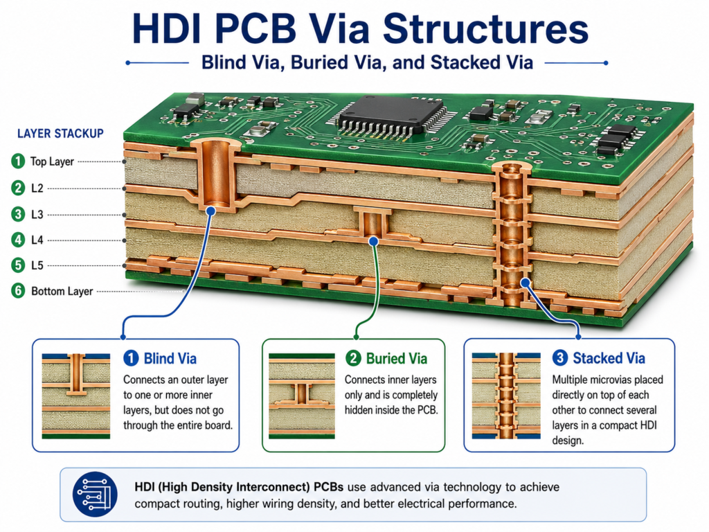
The High Transition: From Through-Holes to Microvias
conventional multilayer layouts: signal moves between layers with standard through-hole vias. Its thinking is more important; slow-moving elevators are drilled from the upper penthouse layer towards the basement.
Also, if a signal requires a hop from Layer 1 to Layer 2, elevator shafts blast on every single floor, permanently covering premium real estate where different components require live
HDI manages that congestion with the use of microvias. That is an agile, microscopic path less than 150 µm wide that only connects the floors that actually need connection to each other, making the rest of the building free for routing.
Architecture of Inner-Layer Shortcuts
For data to flow smoothly, easily, and without hindrance, different types of microvias were made.
Blind Vias:
These vias are made from the external layer and end at some layers and are not seen from the other side of the board.
Buried Vias:
These vias are made from the top layer and seen from the other side of the board easily.
Stacked vs. Staggered Vias:
Stacked vias made directly on top of each other, such as vertical elevator shafts, are incredibly space-efficient but not good for lazy fabricators.
Staggered vias are made on different layers, making them easy to configure during the production process.
Advanced Fabrication techniques
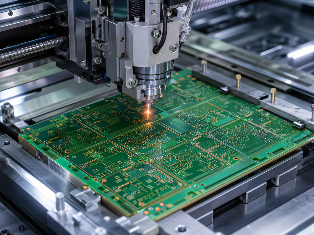
There are difficulties in making high-performance HDI multilayer PCBs with old manufacturing methods that need completely different techniques and engineering methods.
Sequential Laminations:
Standard boards laminated in single cycle. HDI boards needed proper sequential lamination.
Layer-by-layer production
The manufacturer started with solid core layer processing and baked extra layers of dielectric and copper foil in sequence. When every single layer was applied, the laser drilled new microscopic paths before the next layer was applied.
These cycles’ repetition helps make complicated designs, multilayer masterpieces (often classified as 1+N+1 or 2+N+2 structures), that would not be possible for traditional manufacturers.
Laser Drilling
Mechanical drill bits snap when making holes less than 150 µm, compared to HDI based on high-energy ultra-violet (UV) and CO₂ lasers.
These lasers work like small scalpels, vaporizing materials shortly and stopping when they reach the certain copper pad underneath.
Plating and via-in-pad features
When a hole was drilled, it needed coaxing in to conduct electricity.
Chemical Copper Coating:
• A microscopic copper layer was chemically washed over the internal hole walls.
Via-in-Pad Plating (POVIP):
For saving the last mm of area engineering, use the method that covers microvias directly in metallic pads where components are connected.
Manufacturing staff fill holes with special epoxy, plate them with flat copper, and make an accurate smooth surface for surface mount components’ connection.
Why Hardware Designers Are Preferring HDI
Giving Signals a Cleaner, Shorter Path
When the data speed increases, electrical signals do not work like current and are highly faulty at high speeds. If the signal faces a larger through-hole via extra metalwork like a dead-end stub, the result is signal distortion and the generation of electromagnetic noise (EMI).
Microvias manage stubs, providing a high-frequency signal with accurate smoothness and a small running path
Fine-Pitch BGAs
The good processor, memory chip and FPGA currently working in AI and 5G tech features Ball Grid Arrays (BGAs) with hundreds of pins spaced barely $0.4\ mm$ apart.
standard routing technique not squeezed between microscopic pins. HDI’s via-in-pad method helps pins be added into internal layers and makes difficult appearances easily
Weight and reducing dimensions
Double-squeezing the working of each square mm, HDI helps to reduce a 12-layer conventional board to a short-size, highly effective 8-layer HDI option.
Drones, medical devices, and vehicle control units: weight reduction is the best option.
Hidden Faults of High-Density Layouts
Thermal Pressure
When a larger number of components are connected into a small assembly, a confined area where heat is produced accumulates. Since boards are highly compact, they cause high thermal pressure. During design, proper thermal vias should be made, and reliable materials such as high-Tg FR-4 should be used to help the board release heat and remove heat before damaging the silicon.
Microvia Delamination
Copper and fiberglass substrates are not generated equally when heat is supplied. During soldering, they apply reverse force to each other. If manufacturers cut corners, that inner stress causes cracking of microvias and delamination. Finding an HDI PCB manufacturer who knows how to control structure and follows IPC Class 3 standards is best for hidden failures.
Sourcing and Assembly Survival Strategy-
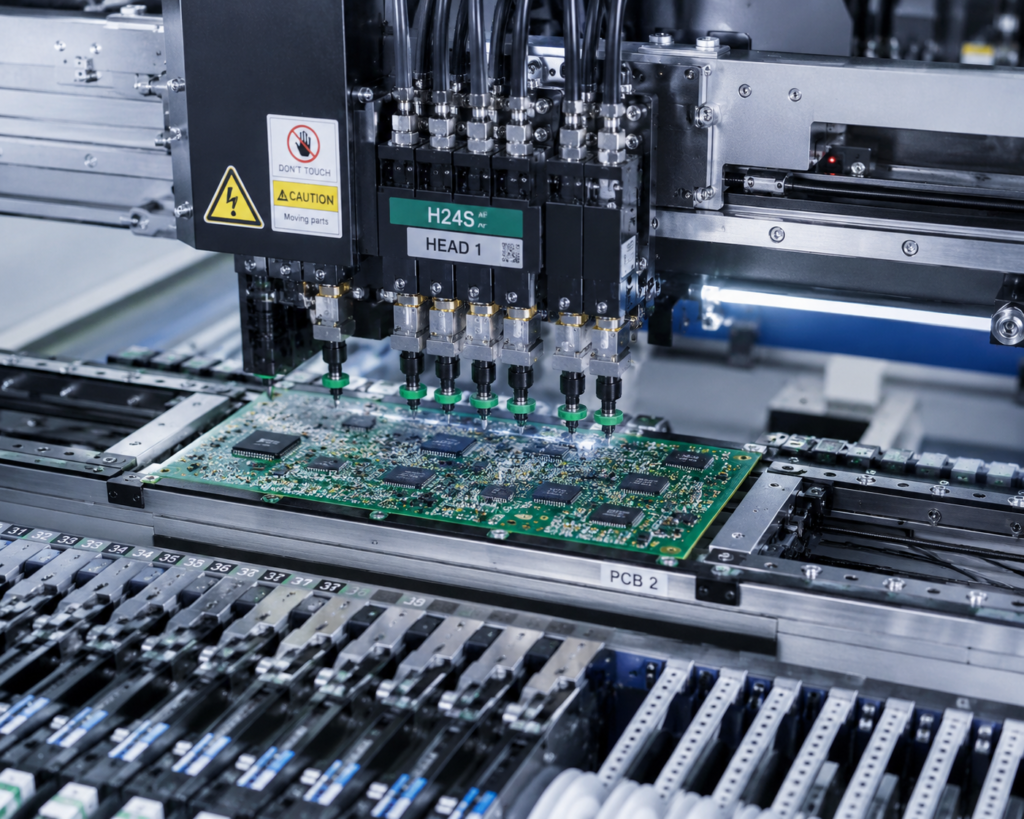
Proper design is helpful for making design reality for a safe and low-cost budget.
Choosing a Fabrication Ally
Designing files needed, sharing experience details and collaborating with a reliable HDI PCB fabrication team during the starting phase of layout saves weeks of frustration. They can run files through Design for Manufacturing (DFM) checks to ensure their lasers and lamination presses can handle your tight tolerances without driving down assembly products.
Solder Reflow Under a Microscope
Assembly of the HDI board required accurate techniques. Through small 01005 components, adjusting mm distance, standard automated pick-and-place machines cause difficulties. HDI PCB assembly services must use state-of-the-art 3D Solder Paste Inspection (SPI) for offering microscopic solder joints that are errorless, with 3D X-Ray (AXI) machines to go deep beneath. BGA chips to check that the hidden connections are solid.
Turnkey Advantage:
Making a project between distinct bare-board manufacturers and assembly houses is best for finding faults. Operating as a unified, end-to-end HDI PCB board supplier that manages the entire lifecycle—from the first laser drill to the final automated optical inspection—enables easy communication, protects small margins, and converts hardware into the real world faster.
Final Thoughts
HDI techniques are a natural evolution for electronic products that need high speed, compact design, and raw computing power. With the following physical requirements of signals following thermal features of material, configure design properly with manufacturing staff that gives details about high-density circuits; you can convert your hardware project into an optimized, highly reliable design.