In modern electronic designs, a rigid-flex PCB stack-up is considered an important technique and advancement. In this technique, a stable structure of rigid boards is configured with the flexibility features of flexible boards. It works like innovative methods that help to make accurate, compact, and reliable electronic circuits and projects for different applications like the vehicle industry, medical devices, etc.
For faultless application of rigid-flex PCB stackups, a proper understanding of the materials used, engineering knowledge, and performance optimization aspects is required. With the advancement in technology, new electronic devices demand miniaturization, so the use of rigid-flex stack-up design is becoming important.
In this tutorial, we will cover the detailed features of rigid-flex stackups and relevant factors. Let’s get started.
What Are Rigid-Flex PCBs
- A rigid-flex board comes with the combined features of rigid and flexible PCBs in circuit board assembly.
- These come with different layers made with flexible polyimide substrate and rigid FR4 materials in a single unit.
- This mixture of boards helps to reduce the number of connectors used, making a tight structure with high reliability.
- Their compact design makes these boards lightweight and allows them to be installed in compact locations and also allows them to handle harsh conditions.
- In this hybrid design, rigid parts are used for circuit component connections and flexible parts for bending, so these boards are used in circuits of mobile phones, aviation systems, and medical devices.

Introduction to Rigid-Flex PCB Stackups
- Rigid-flex PCB stackup is basically a layered assembly or structure that is made with conductive layers and insulating and bonding material layers.
- Stackup comes with FR4 material layers that are rigid and provide support to the complete structure and flexible layers made with polyimide that provide bending features to the board design.
- Let’s suppose an example of a commonly used four-layer rigid-flexible board stackup that is made with a combination of two rigid material layers connected between two flexible material layers, making a sandwich assembly. Each layer comes with copper tracing that performs signal routing.
- The design of layers must be such that it provides good flexible features with electrical performance and mechanical support.
- Through proper stackup design, we get a quality signal and controlled impedance, with controlled signal losses and crosstalk.
| Layers | Material | Operations |
| Upper Rigid Layer | FR4 material | electronic components connections |
| Flex Layer 1 | Polyimide | Routing of signal |
| Flex Layer 2 | Polyimide | Routing of signal |
| lower Rigid Layer | FR4 | Connectors |
Rigid-Flex PCB Manufacturing Materials
There are different materials used for making rigid-flex PCB stackups; one must use materials that are cost-effective but affect the performance and durability of the board.
Some materials used for rigid-flex board stackups are as follows.
Flexible Materials
- Polyimide is used as a flexible material that has good tensile strength and also handles bending features. Polyimide has features to operate well in harsh conditions, like handling temperatures of about 250 degrees.
- Some boards needed low thickness with high flexibility, where adhesive-less polyimide materials were used.
Rigid Materials
- The rigid part of the stackup is made with glass-reinforced epoxy laminates that are strong and remain stable for high-temperature conditions. FR4 also uses rigid materials since its dielectric constant is 4.5, which helps it to be used in different applications.
- Some advanced projects where high frequency is needed, Rogers laminates are used as rigid materials that reduce signal losses.
Adhesives
- For making a strong connection between rigid and flexible layers, adhesives are used. Epoxy adhesive is commonly used, but for good thermal ability of boards, an adhesive-less design is used.
- But it is based on the structure of boards for handling thermal and mechanical stress.
Construction rules of rigid flex PCB Stackup
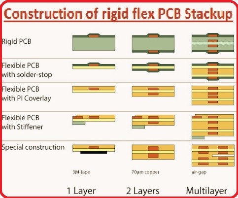
There is a difference in rigid-flex PCB stackup and conventional PCB boards in terms of material and design features.
A rigid-flex stackup comes with alternative rigid and flexible material parts that, when connected during the lamination process, make a single assembly.
For mechanical support, FR4 rigid materials are employed where circuit components are mounted, and they also cause heat dissipation.
On this layer, components are connected through the thrughfollowing smt and through-hole component connection techniques with maintenance of dimensions and mechanical stress.
Change from rigid to flexible layers follows techniques that help to manage stress and provide electrical continuity during the working life of the board.
Flexible parts use polyimide films with a thickness range of 12 to 125 um based on the number of layers.
The flexible part of the board uses annealed copper conductors that provide highly flexible features.
The copper conductors in flexible regions utilize rolled annealed copper for superior flexibility and fatigue resistance compared to electrodeposited copper used in rigid sections.
Rigid-Flex PCB Stackup
- Rigid-flex PCB stackups make reliable boards and have low failure points, since they come with fewer connectors and solder joints.
- It makes thinner boards, which are low weight and compact in design.
- It provides proper heat dissipation for high-performance projects.
- It has a high aspect ratio, so it is preferred in complicated and high-density interconnect (HDI) designs.
- It comes with a 3D flexible structure, so it easily bends and folds in low-space applications.
Rigid-Flex PCB Manufacturing Process
The manufacturing process of a rigid-flex board comes with different steps that are explained here.
Design step
- In the first step of all, a detailed stackup design is made, where the number of layers of materials used and their types and thickness are defined.
- Different software used for designing rigid-flex boards that make simulation of signal quality and mechanical stress management.
- Designing a rigid-flex board is difficult since it needs three-dimensional spaces for rigid-flex designs.
- Normally, the thickness value of flex layers in board design is 0.002 inches, and the rigid layer thickness is 0.062 inches.
Prepare Material
- In this step, raw materials are required for the board and cut into the required shape. FR4 is a rigid material that has copper foil laminations, and for uniform thickness, polyimide is applied as a flexible material.
- prepreg layers used for material bonding purposes
Lamination process
- For layer stacking and strong bonding, high pressure and temperature are applied in the lamination process to make strong bonding. This process ensures rigid and flexible parts without any faults or contaminations
Drilling
- Holes are made on the board for making vias to connect components. For making holes,, laser drilling is used, which makes accurate holes.
- After drilling holes in the flex pattern,, copper isis deposited in the holes, a process known as through-hole plating ,where copper is chemically plated.
- If your board is high-density, it comes with a larger number of components and microvias used.
Etching and circuit pattern
- for making the required cirucit design pattern, copper layers are etched. for making traces about 0.003 inches, UV light is applied to copper through a mask in photolithography.
- After that coverlay is applied on the upper and lower flex substrate layers. normally coverlay protection layers made with polyimide materials
Testing and assembly
- To make sure of board continuity and insulation resistance, electrical tests are performed, but before testing methods, surface finishes such as ENIG (Electroless Nickel Immersion Gold) are applied to resist corrosion.
- For monitoring the flexible part of the board handling certain cycles, bend tests are performed that ensure the flexible part provides about 100,000 bends for different applications.
Challenges for rigid flex board manufacturing
- To make sure of board continuity and insulation resistance, electrical tests are performed, but before testing methods, surface finishes such as ENIG (Electroless Nickel Immersion Gold) are applied to resist corrosion.
- For monitoring the flexible part of the board handling certain cycles, bend tests are performed that ensure the flexible part provides about 100,000 bends for different applications.
Design Factors of Rigid-Flex PCB Stackup
There are some factors we must follow for designing rigid-flex PCB stackups for reliable working performance.
Material
- Use high-quality materials for board manufacturing of a rigid-flex design, with FR4 in the rigid part and flexible layers made from polyimide, resulting in a flexible, durable structure.
Bending Radius:
- For controlling the cracking of the board, use the required bend radius, normally ten times the flex part thickness bending radius used.
Via
- For making a reliable structure, staggered vias are used in a flexible board layer.
Heat management
- In projects where high power used, causing high heat, for proper heat management, thermal vias and heat sinks are used on the rigid layer.
Maintain Signal Integrity:
- Use proper tracing spacing and width that manages signal losses.
Rigid Flex Stack Up vs. conventional Rigid/Flex PCBs
Conclusion
Rigid flexboards are compact in design and make reliable structures, but all occur through proper design and manufacturing techniques. We can make high-performance boards by using proper rigid-flex PCB material, accurate manufacturing methods, and applying proper design rules.