The electronics industry is fast-growing; with that, manufacturers are finding fast, effective, and low-cost methods for making printed circuit boards. Requirements for rapid product development and customization, and fast-growing new manufacturing methods such as 3D printing, are becoming common for long-established processes of traditional PCB etching.
While conventional PCB fabrication remains the industry standard for commercial manufacturing, 3D printing is opening new chances for rapid prototyping, complex design, and on-demand manufacturing. Understanding the strengths and limitations of each method helps engineers, startups, and manufacturers use the most effective production techniques for their specific applications.
What is traditional PCB etching?
Traditional PCB manufacturing follows subtractive manufacturing methods. The process starts with a copper-clad laminate, where undesired copper is removed with an etching solution, leaving traces that form an electrical circuit.
The manufacturing workflow comes with different phases, such as PCB design, photolithography, chemical etching, drilling, plating, solder mask application, surface finishing, and quality inspection.
Advanced manufacturing features employ high-level automated devices for getting accuracy and repeatability.
That method has been refined for many years and is the best option for making different projects, like consumer electronics and automotive systems, to industrial devices and medical devices.
Its features help engineers to get high-level tolerances, constant electrical features, and production volumes while maintaining competitive costs.
What Is 3D PCB Printing?
3D PCB printing is an additive manufacturing process that makes electronic circuits in layer form compared to removing material from a copper sheet.
Special printers deposit conductive inks with insulating materials for making functional circuit boards from digital designs.
Compared to traditional manufacturing, which needs different manufacturing phases and special tools, different features of PCB production can be integrated into a single workflow.
Engineers can quickly modify digital files and print updated prototypes without creating new masks or production tooling.
Either technology is growing fast or advancements in conductive material printer resolution and multi-material printing continue to expand its features across research, education, aerospace, healthcare, and rapid product development.
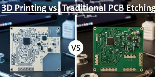
Differences Between 3D PCB Printing and Traditional Etching
Manufacturing Speed
The main difference is two manufacturing techniques: manufacturing speed.
Conventional PCB manufacturing follows different processing phases and quality inspection before finishing the board. For manufacturing runs, that structured workflow offers proper and repeatable results.
But design revision needed an extra manufacturing cycle at high speed. 3D printing reduces time for the prototyping process.
Designers can move from a finished CAD model into a physical prototype in hours compared to taking time for days or weeks for fabrication and shipping.
That rapid turnaround helps engineers test concepts, find design errors, and iterate during product development.
For companies that prefer innovation, faster iteration often converts into reduced development costs and shorter time-to-market.
Cost
cost based on manufacturing volume and project demand. Conventional PCB board manufacturing gets features from economies of scale. Once production tooling and setup are complete, the cost per board reduces substantially as order quantities increase.
This makes conventional manufacturing low cost for medium- and high-volume manufacturing. For low-volume manufacturing, research projects, and prototype development, these savings can offset the higher material costs.
Developing different design variations to get that 3D printing to minimize competitive manufacturing costs irrespective of high individual manufacturing charges
Flexibility of design
Advanced electronics products are now shifting towards shrink design and becoming sophisticated. This factor offers high demands on PCB design.
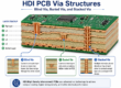
Conventional manufacturing compatible high-complexity multiverter boards with high accuracy. Advanced manufacturing methods help engineers to make fine traces, high-density interconnects, blind vias, buried vias, and different features needed for today’s electronics.
3D printing adds different flexible levels. Engineers can make unconventional designs, curved surfaces, embedded components, and customised structures that can be difficult, sometimes not easy, to construct with standard etching processes.
These features are preferred for wearable devices, the aviation industry, medical devices and customised electronic products, where special form factors are as important as electrical performance.
Material Usage and Environmental Factors
Sustainability is becoming important for electronics manufacturing. Traditional PCB fabrication is a subtractive process, meaning significant amounts of chemical solutions are applied to remove unwanted material. Manufacturers have highly advanced waste management and recycling practices, but chemical processing is an important part of production.
Since 3D printing makes objects where material is needed, that normally makes less material wastage. Additive production minimises use of certain chemical processing steps, making it an attractive feature for organisations pursuing more sustainable manufacturing practices.
Environmental footprint based on conductive materials, polymers, printer energy usage, and recycling techniques used during production.
Production Quality and Reliability
For factors where reliability is important, conventional board manufacturing continues for certain advantages.
Conventional manufacturing has many years of good performance in different industries that need certain durability.
These include automotive electronics, telecommunications, defense, aerospace, and medical equipment. Manufacturers use certain quality standards for electrical consistency and long-term reliability.
3D printing technology has advanced features printed with conductive material not fulfilling electrical conductivity, mechanical strength, or long-term durability got through conventional copper manufacturing in every application.
Since materials science is fast-growing, the performance gap is reducing, but conventional manufacturing is the best option for important projects.
Scalability
Manufacturing volume is the main factor for manufacturing techniques. Conventional PCB etching is used for large-scale manufacturing. Automated manufacturing lines can produce thousands or millions of the same boards through proper consistency and low per-unit costs.
3D printing is growing for low manufacturing and customization. Every printed board can be modified without variable production tooling, making the technology best for personalized products, research, proof-of-concept designs, and specialized industrial applications.
For businesses producing limited factors or customized electronics, additive manufacturing offers flexibility that conventional manufacturing cannot easily match.
Applications of Traditional Etching vs. 3D Printing
Each manufacturing method is used for different needs within the electronics industry.
Traditional PCB etching used for
- Consumer electronics
- Automotive systems
- Medical equipment
- Industrial automation
- Telecommunications
- Large-scale commercial production
Meanwhile, 3D PCB printing part of:
- Rapid prototyping
- University research
- Product development
- Aerospace innovation
- Wearable technology
- Internet of Things (IoT) devices
- Custom electronics
- Low-volume manufacturing
Compared to competing directly, these methods often complement each other during different phases of product development.
Future of PCB Manufacturing
The future is unlikely to be defined by one manufacturing technique’s replacement for the other. Instead, hybrid workflows are growing fast. Different engineering teams apply 3D printing at the time of early design and testing since it provides rapid experimentation and fast design revisions. Once the design has been validated, manufacturing shifts to traditional PCB fabrication for large-scale manufacturing.
Meanwhile, ongoing advances in features in conductive inks, printable electronics, flexible substrates, and multi-material additive manufacturing continue to grow the field of 3D-printed electronics. Researchers are finding methods to print complete electronic systems, such as conductive pathways, sensors, antennas, and structural components in a single manufacturing process.
As these methods mature, manufacturers will come up with options for balancing speed, cost, customization, and performance.
Conclusion
Both 3D PCB printing and conventional PCB etching play highly featured roles for advanced electronics manufacturing. Traditional manufacturing continues to offer the precision, reliability, and scalability required for commercial manufacturing, making it the building block of today’s electronics industry.
At the same time, 3D printing is shifting how engineers prototype and make new products by enabling faster variations, greater design freedom, and efficient low-volume manufacturing. Although it has not yet replaced conventional manufacturing for bulk production, its effects continue to grow as materials and printing technologies evolve.
For many companies, the smartest method is not using one method over the other but combining both. Rapid prototyping through 3D printing, followed by conventional manufacturing for large-scale production, helps businesses to grow innovation while maintaining the quality and reliability expected from modern electronic products.